AOI, X-ray, Flying Probe, ICT or Functional Test? Choosing the Right Check
Each inspection and test method sees some faults and misses others. Here is what AOI, X-ray, flying probe, ICT and functional test can really catch, and how to choose by volume and risk.
Microplacer team · 15 November 2026 · 5 min read
 Quality & Testing
Every test method has a blind spot. A board can pass a camera check and still have an open joint under a BGA. It can pass an electrical test and still not boot. The aim is not to buy every test, but to pick the mix that covers the faults most likely on your design.
Inspection vs test: what each answers
First, separate the questions. Inspection asks “was this built correctly?” It looks at parts and solder joints without powering anything. Electrical test asks “is the circuit connected and are the parts what they should be?” It measures opens, shorts and component values. Functional test asks “does the product do its job?” It powers the board and checks behaviour.
Because the questions differ, no single method replaces the others. A sound plan draws on at least two of these groups.
AOI for visible solder and placement defects
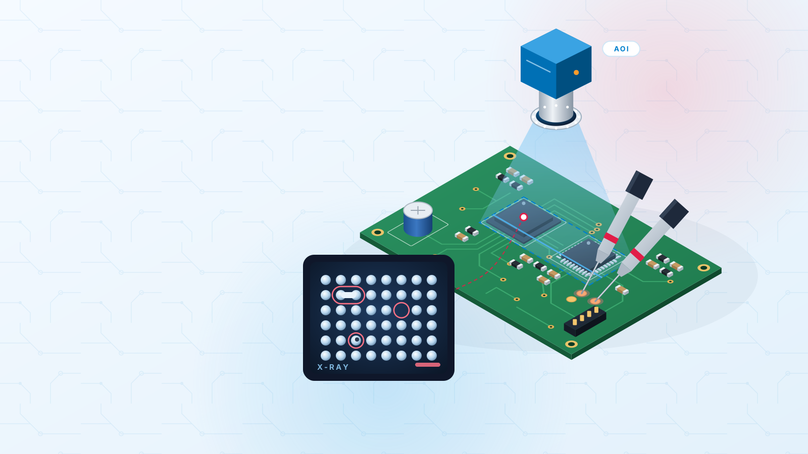
Automated optical inspection uses cameras and lighting to compare each assembled board against what the placement data says should be there. It is fast, it needs no contact with the board, and it fits naturally right after reflow, which makes it the workhorse for SMT lines.
- Good at: missing or extra parts, wrong rotation or polarity (when the part has a visible mark), shifted or skewed parts, tombstoned chips, bridges between visible leads, too little or too much solder in visible fillets.
- Blind to: joints the camera cannot reach because a package sits on top of them (BGA, LGA, QFN thermal pads), trapped gas inside a joint, a poorly wetted joint whose surface still looks smooth, and two passives that look the same but carry different values.
AOI is only as sharp as the data behind it. The machine learns where each part belongs and how it should face from your centroid file and BOM, so wrong rotations or missing reference designators mean more false calls and more chances for a real defect to slip through.
X-ray for BGA and hidden joints
When the solder joint is underneath the part, cameras cannot help. X-ray inspection sees through the package and shows the solder itself. It is the standard way to check BGAs, CSPs, LGAs and QFN thermal pads for bridging, missing balls, misalignment and voiding.
Some voiding in reflowed solder is normal. Acceptance limits are defined in IPC-A-610 and, for BGAs, IPC-7095; limits for large thermal pads are often set by the part maker or the customer. If voiding matters for heat transfer in your design, agree the limit before production rather than after. Also note that a simple top-down image may not reveal every open; angled views help with tricky faults like head-in-pillow.
Flying probe vs ICT: fixtureless flexibility vs volume speed
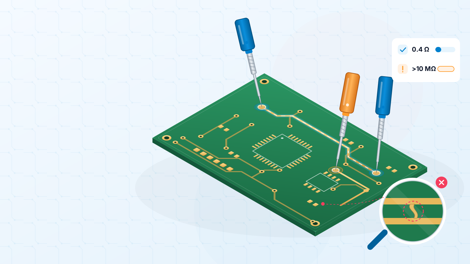
Both methods put metal probes on the board and take measurements with it mostly unpowered. They confirm that nets connect where they should and nowhere else, that resistors and capacitors are close to their rated values, and that diodes face the right way. Where they differ is in how the probes reach the board.
- Flying probe uses a few moving probes that hop from point to point. There is no fixture, only a program generated from CAD data, so set-up cost is low and design changes are easy. The trade-off is speed: a board can take minutes.
- In-circuit test (ICT) presses a custom bed-of-nails fixture onto every test point at once. Each board takes seconds, but the fixture costs money and usually needs rework when the layout changes.
In short: flying probe for prototypes, small batches and designs still changing; ICT for stable designs built in volume. Either way, plan accessible test points on your nets early. IPC-2221 includes testability guidance worth reading before layout.
Functional test: does the product actually work
Functional test (often called FCT) switches the board on and uses it the way the end user would: check the supply voltages, load the firmware, talk to the interfaces, exercise the outputs. Of all the methods here, it alone can expose design and firmware mistakes, and it is the closest thing to what your customer will experience.
Its weakness is diagnosis: a failed functional test tells you something is wrong, not which joint or part caused it. That is why it works best on top of inspection and electrical test, not instead of them.
Comparison table and choosing by volume and risk
| Method | Finds best | Misses | Best fit |
|---|---|---|---|
| AOI | Placement, polarity, visible solder faults | Hidden joints, part values, function | Every SMT build |
| X-ray | BGA/LGA/QFN joints, voids, hidden bridges | Part values, function | Boards with hidden-joint packages |
| Flying probe | Opens, shorts, values, diode direction | Firmware, timing, behaviour | Prototypes and small to medium batches |
| ICT | Same as flying probe, much faster | Firmware, timing, behaviour | Stable designs in volume |
| Functional test | Does the product work | Root cause of the fault | Anything going to a customer |
To pick your mix, walk through these questions:
- 1Does the board have BGA, LGA or QFN parts? If yes, plan for X-ray on top of AOI.
- 2How many boards, and will the design change? A few boards or frequent revisions point to flying probe; a frozen design in volume can justify an ICT fixture.
- 3What does a field failure cost? Anything safety-related or hard to repair deserves a functional test on every unit.
- 4Have you added test points and kept polarity marks visible? Testable design makes every method cheaper and more reliable.
Next step
For more detail on each method, read our PCBA testing and inspection guide. If your board has BGA, LGA or 0201 parts, it goes to engineering review before the assembly price is confirmed — a good moment to tell us which checks you expect. You can also see what we offer on our testing and inspection service page.
#aoi#x-ray-inspection#flying-probe#ict#functional-test#pcba-testing
Get an instant PCB quote