Assembly-Ready Files: The Gerber, BOM and Pick-and-Place Checklist
A practical checklist for sending a complete, consistent PCBA package, so the instant price and the finished boards both match your design.
Microplacer team · 15 November 2026 · 5 min read
 PCB Assembly
Most assembly delays start in a zip file, not on the line: a missing paste layer, a BOM that says R12 where the placement file says R21, or an unchecked rotation column. A complete, consistent package means the online price matches the board you designed.
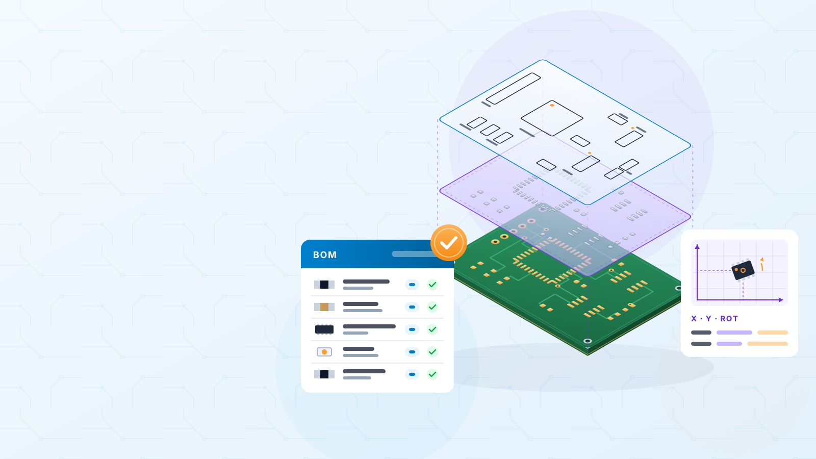
This checklist walks through the three files every PCB assembly order needs (Gerber, BOM and pick-and-place) and the small details that keep them telling the same story.
Why the PCBA instant price comes from solder pads
The effort in assembly scales with the joints that must be printed, placed and soldered. That is why our online calculator works out the PCBA price from how many solder pads each board has and how many boards you order. Surface-mount pads are taken from the paste layers of the side or sides being assembled; through-hole pads come from the plated holes in the drill data.
In other words, your Gerber does double duty: it builds the board and it feeds the assembly price. Leave out the paste layers and the pad count can only be approximated from the solder mask, flagged as an estimate for you to correct by hand. Include them and the count is right first time.
Gerber layers to include (yes, the paste layers too)
For an assembly order, one zip should contain all of the following, exported from the final revision of the design:
| Layer / file | Why assembly needs it |
|---|---|
| Copper (top, bottom, inner) | Defines the pads and the board itself. |
| Solder mask (top, bottom) | Shows where pads are exposed for soldering. |
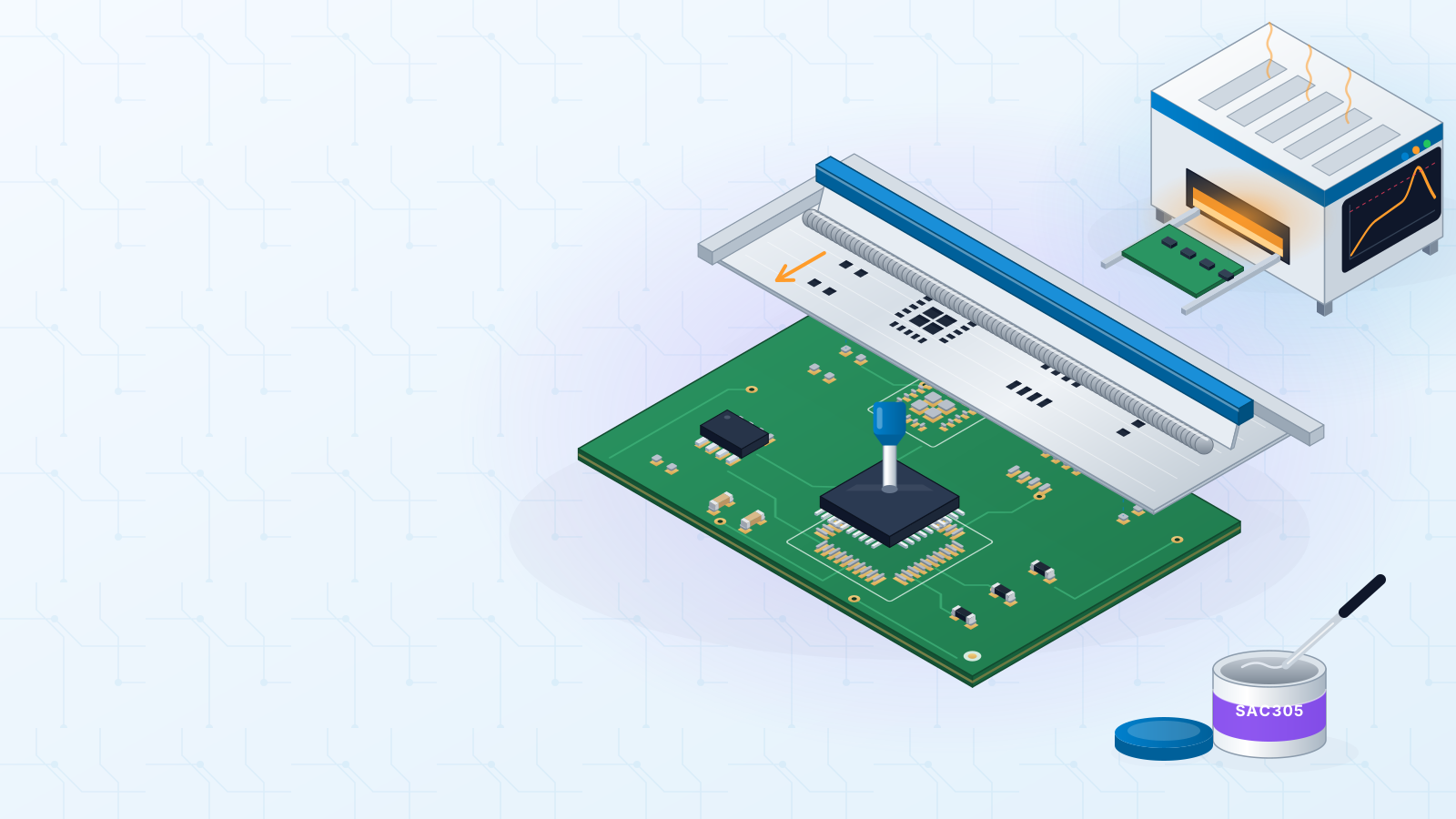
| Solder paste (top, bottom) | Becomes the stencil and drives the SMD pad count. The most commonly forgotten layer. |
| Silkscreen (top, bottom) | Designators, polarity marks and pin 1 indicators that operators and inspectors rely on. |
| Board outline | A single closed contour; the board size is read from it. |
| Drill files (Excellon) | Plated and non-plated holes; through-hole pads are counted from these. |
We read the board size from the Gerber automatically, but please confirm it matches what you expect. A stray line outside the outline is enough to make a board look bigger than it is.
BOM columns that prevent confusion
Think of the BOM as one line per kind of part, not per individual part. Fill in these columns and most follow-up emails never need to be written:
- Designators — every reference on the board for that part (R1, R2, R7), spelled exactly as on the silkscreen.
- Quantity per board — and it should equal the number of designators in that row.
- Manufacturer part number (MPN) — the single most useful column. A value such as “10k” is not enough to buy the right part.
- Value and package — a quick cross-check that the part fits the footprint (0603 part on an 0603 footprint).
- DNP / do not place — mark unfitted parts clearly in the BOM rather than just deleting the row, so nobody wonders whether it was forgotten.
Pick-and-place file: units, rotation and origin
The pick-and-place file (also called centroid, CPL or XY file) lists each SMD part with its centre position, rotation and side. Three details cause most of the trouble:
- Units — state them. A file in mils read as millimetres puts every part in the wrong place. Exporting in mm with the unit in the header is safest.
- Rotation — angles are in degrees, but CAD libraries do not all use the same zero orientation. Polarised parts (diodes, ICs, electrolytics) are where a wrong angle matters, so make polarity and pin 1 visible on the silkscreen as a reference.
- Origin and side — coordinates are measured from the board origin, so keep it consistent with the Gerber. Include a layer column (Top / Bottom) and both sides in the file if you assemble both.
Keep BOM, CPL and Gerber in sync
Problems usually appear between files after a late change: a part renumbered, a footprint swapped, or a DNP resistor still in the placement file. The fix is discipline:
- 1Export all three files in the same session, from the same final revision.
- 2Confirm that the BOM, the placement file and the silkscreen use exactly the same reference designators.
- 3Make sure every DNP part is marked in the BOM and that you know whether it still appears in the placement file.
- 4Name the files with the board name and revision so an old BOM never sneaks into a new zip.
Our engineers check your files before production and compare any production notes with our options, but a consistent package still means fewer questions.
Final pre-upload checklist
| Check | Done? |
|---|---|
| One zip, final revision: every Gerber layer plus drill data | ☐ |
| Paste layer present for every side being assembled | ☐ |
| Outline forms one closed shape and the detected size looks right | ☐ |
| Every BOM line carries designators, quantity, MPN, package and any DNP flag | ☐ |
| Placement file states units and includes rotation, side and the same designators | ☐ |
| Diodes, ICs and electrolytics show their orientation in the silkscreen | ☐ |
| Any BGA, LGA or 0201 parts declared, since they go to engineering review | ☐ |
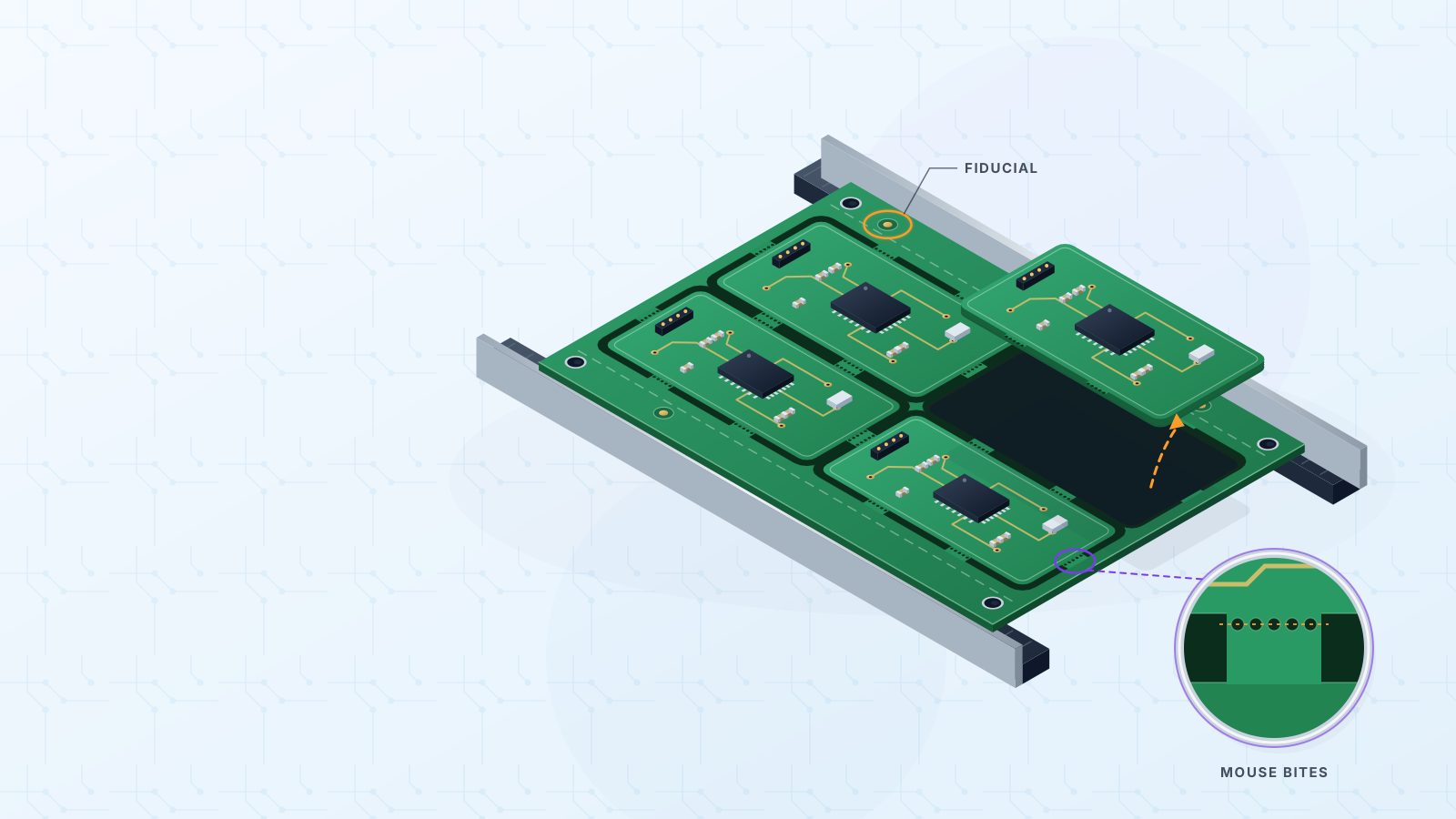
| A panel supplied, or “Panel by Microplacer” chosen (PCBA runs in panels only) | ☐ |
On quantity: 5 to 50 boards carry no stencil charge, and from 55 boards a one-time shared stencil appears in the quote. In both cases the stencil is cut from the paste layers you send.
Next step
Ready to export? Our file preparation guide shows where the export options live in KiCad, Altium, EasyEDA and Eagle, and the assembly quote FAQ covers pad counts, stencils and panels. Then upload your package for an instant PCBA price.
#pcb-assembly#gerber-files#bom#pick-and-place#checklist
Get an instant PCB quote