Using BGA, QFN or 0201 Parts? What to Expect When You Order Assembly
Boards with hidden-joint and tiny parts go to engineering review instead of an instant price. Here is why, how to design pads, vias and finish for them, and how they are inspected.
Microplacer team · 15 November 2026 · 5 min read
 PCB Assembly
Your layout passes DRC, with a BGA processor and a ring of 0201 capacitors around it. You upload the files expecting an instant assembly price, and the quote says engineering review instead. Nothing has gone wrong: some joints on your board are hidden or very small. Here is what the review is for, and how to make it painless.
Why these parts skip the instant price
Our online PCBA price is built from two things: how many solder pads each board has, and how many boards you want. For resistors, SOICs and connectors that fairly reflects the work. A BGA does not: it can need a thinner stencil, careful profiling, X-ray and moisture-controlled handling, none of which a pad count shows.
So when the calculator sees BGA, LGA or 0201 parts, it hands the board to an engineer rather than showing a figure that could change later. The engineer checks packages, footprints, paste and inspection needs, then confirms a price. QFNs and fine-pitch QFPs are less demanding because some of each joint can be seen, but every order still has its files checked by our engineers before production.
| Package | Joint location | Typical failure modes |
|---|---|---|
| BGA | Solder spheres in a grid beneath the part | Opens, shorts, voids, head-in-pillow, warpage |
| LGA | Flat lands beneath the part, no spheres | Almost no stand-off, so paste volume and flatness are critical |
| QFN / DFN | Perimeter lands plus a big centre pad | Voids in the centre pad, part floating or tilting |
| 0201 chips | Two very small terminations | Tombstoning, skew, starved joints |
Get the footprint right first
The most reliable way to avoid trouble is to start from the land pattern in the component datasheet, built to IPC-7351 conventions, instead of a library footprint nobody has checked. For BGAs, non-solder-mask-defined (copper-defined) pads are the usual starting point, unless the datasheet asks for something different.
Vias deserve a second look. A dog-bone fanout, where a short trace leads from each ball to a via sitting between the pads, normally works fine with ordinary tented vias. Put the via inside the pad, though, and an open hole will drain solder away from the ball and release gas into the joint. Any via-in-pad should be filled and capped; our online calculator lists epoxy and copper-paste filled and capped options for this.
The centre pad of a QFN has its own trick. Printing it through one big opening deposits too much paste, so the part can float and flux gas has nowhere to go. Dividing that opening into a grid of smaller windows in the paste layer solves both. If your paste layer does not do this yet, ask for it in your notes.
Flat pads, flat boards
Tiny deposits need an even surface. HASL leaves pads slightly rounded, which is harmless for big parts but can tip a 0201 or give an uneven print under an LGA. ENIG is the common pick for area-array boards because it is flat and keeps well in storage. OSP is flat and cheaper too, as long as the boards are assembled fairly soon after delivery.
The board must stay flat too: bow or twist in the oven can lift BGA corners off the paste as it melts. Balanced copper and a symmetrical stack-up help. Compare the finishes in our surface finish guide.
Seeing joints you cannot see
A camera only sees the top of the board, so hidden joints are checked with X-ray. Solder blocks X-rays far better than the plastic body or the laminate, which makes every ball appear as a dark circle. Looking straight down shows shorts, missing balls and voids well; tilted views reveal ball shape and help when parts on the opposite side overlap the image.
It is not a perfect test. A ball that sat on the paste without ever fusing to it (head-in-pillow), or a joint that wetted poorly, can still look normal on screen. That is why X-ray is paired with electrical and functional testing. If you need X-ray on particular parts, a maximum void level or a specific IPC-A-610 class, put it in your notes; our engineers read production notes and compare them with what we offer.
Plan for rework, but do not rely on it
A short between QFP leads takes a minute with an iron. A short under a BGA means lifting the whole package off with controlled heat, clearing the pads, then fitting a fresh or reballed part and inspecting it again. It often works, but every heat cycle stresses pads and laminate, and a site can only be reworked a few times.
- Give large BGAs some breathing room so a rework nozzle and angled X-ray views can reach them.
- Keep tall parts out of the area directly around a BGA.
- Expect underfilled parts to be very hard to remove.
- Read repair and rework to see what is realistic.
Before you press upload
- 1Footprints taken from the datasheet; pin 1 or ball A1 marked on the silkscreen and any assembly drawing.
- 2ENIG selected in the calculator, or OSP if assembly follows quickly.
- 3Every via that sits in a pad filled and capped.
- 4QFN centre pads split into windows in the paste layer, or a note asking for it.
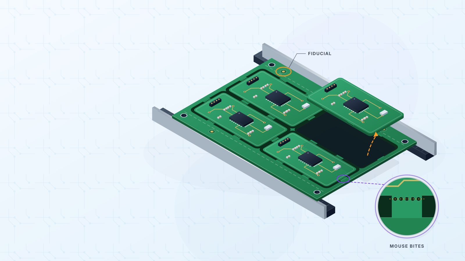
- 5Local fiducials beside large fine-pitch parts, each with a clear area around it.
- 6Top and bottom paste layers, a BOM with full manufacturer part numbers, and a placement file with checked rotations.
- 7Notes covering inspection needs, moisture-sensitive packages and any parts you will supply.
Want the full technical picture? Our BGA and fine-pitch assembly guide and design for assembly guide go deeper. When your files are ready, upload them and our engineers will pick it up from there.
#bga#qfn#fine-pitch#x-ray-inspection#design-for-assembly
Get an instant PCB quote