Controlled Impedance for First-Timers: Stack-up, Traces and What to Tell Your Fab
Adding USB, Ethernet, DDR or RF for the first time? Learn when impedance matters, what sets it, and how to write clear impedance notes for your fab.
Microplacer team · 15 November 2026 · 4 min read
 PCB Design
Your last few boards were simple microcontroller projects, and now the new design has a USB port, an Ethernet jack or a 2.4 GHz antenna. Suddenly the datasheet talks about "90 Ω differential" and you are not sure what to do with that number. Here is a practical walk-through: when impedance really matters, what sets it, and how to tell your fab exactly what you need.
Signs your design needs controlled impedance
Think of the rising edge of a signal as a wave moving down the trace. If the trace is short, the whole thing switches at almost the same instant and it behaves like a simple wire. If the trace is longer than roughly a sixth of the distance that edge covers while it rises, the far end lags behind, the trace starts acting as a transmission line, and any mismatch with the driver or receiver shows up as reflections and ringing. Fast edges matter more than clock speed: a 20 MHz clock with a 1 ns edge still carries energy into the hundreds of megahertz.
You probably need controlled impedance if any of these are on your board:
| Interface | Commonly used target | Line type |
|---|---|---|
| USB 2.0 / 3.x | 90 Ω | Differential pair |
| Ethernet (PHY to magnetics) | 100 Ω | Differential pairs |
| HDMI, LVDS, MIPI, PCIe | Roughly 85–100 Ω | Differential pairs |
| DDR memory | Often 40–50 Ω data, 80–100 Ω clock/strobe | Both |
| RF feed to antenna or connector | 50 Ω | Single-ended |
Treat these as starting points only. The number that counts is the one in your transceiver's datasheet or its layout application note.
How stack-up, dielectric and trace geometry set impedance
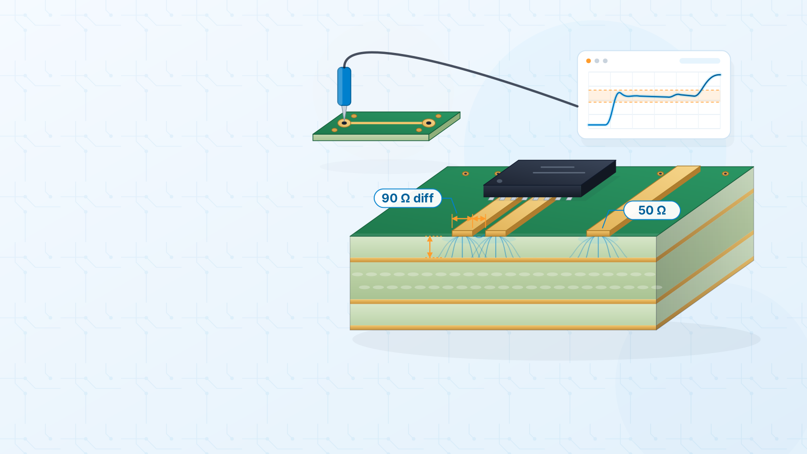
Impedance is not a property of the trace alone; it comes from the trace and the copper plane under it. The main things that set it are:
- Trace width — wider traces give lower impedance.
- Dielectric height — the distance from the trace to its reference plane. A bigger gap raises impedance.
- Dielectric constant (Dk) of the laminate — a higher Dk lowers impedance.
- Copper thickness — thicker copper lowers impedance slightly, which is why you choose copper weight before calculating widths.
- For differential pairs, the gap between the two traces — a tighter gap lowers the differential impedance.
The dielectric height comes from the cores and prepregs in your stack-up, which is why a 2-layer 1.6 mm board is a poor fit: the plane is about 1.5 mm away, so a 50 Ω or 90 Ω line ends up impractically wide. On a 4-layer board with a ground plane on layer 2 just under the top layer, the same targets work with sensible trace widths. Outer-layer traces over one plane are called microstrip; inner traces between two planes are stripline.
Reference planes, return paths and avoiding plane splits
Every fast signal has a return current that flows in the plane directly below it. Your impedance calculation assumes that plane is there and unbroken, so protect it:
- Route fast nets on a layer right next to a solid ground plane.
- Never run a fast trace across a gap or slot in its reference plane — re-route instead.
- Check plane layers under connectors and BGAs, where rows of via clearances can merge into a hidden slot.
- When a signal changes layers, place a ground via next to the signal via so the return current can follow.
- Keep fast traces several dielectric heights away from the edge of the plane.
Material choice for higher-speed and RF work
Standard FR-4 is fine for most first designs with USB 2.0, Ethernet and short RF traces from a module or chip to its antenna — if the chip vendor's reference design uses FR-4, you usually can too. Its weakness is that Dk varies a little between builds and losses grow with frequency. Long multi-gigabit channels may call for a mid- or low-loss laminate, and distributed RF structures such as filters, couplers and patch antennas are normally designed on dedicated RF laminates with a tightly controlled Dk. Specify materials by property (IPC-4101 for rigid laminates, IPC-4103 for high-speed and high-frequency materials) rather than by brand, and expect an engineer to review anything beyond FR-4.
How to write impedance requirements in your fab notes
Vague notes like "USB lines impedance controlled" leave your fab guessing. Give them a short, complete list:
- 1The target and tolerance, e.g. "90 Ω differential ±10%" or "50 Ω single-ended ±10%".
- 2The copper layer each controlled trace sits on (L1, L3 and so on).
- 3Trace width, and for pairs the gap, exactly as drawn in your Gerber.
- 4The reference plane layer(s) for each controlled trace.
- 5For coplanar RF lines, the gap from the trace to the surrounding ground pour.
- 6The stack-up you assumed in your calculator: dielectric heights, Dk and copper weights.
Add these lines as a text file or fabrication drawing in the zip you upload, and give the controlled nets their own net class in CAD so they are easy to find.
Common mistakes: assuming default stack-up, ignoring tolerance
- Calculating widths with a made-up dielectric height. Your CAD tool cannot know the real build; a stack-up that cannot be made will miss its target.
- Assuming the default build is controlled. Without an impedance request, a board is built to a general stack-up, not to your numbers.
- Leaving out the tolerance. Laminate, resin flow and etching all vary, so around ±10% is a common industry figure; tighter needs discussion up front.
- Finishing routing first and asking about the stack-up later. Confirm dielectric heights before you route, or you may have to redo every pair.
- Forgetting the return path: perfect widths over a split plane still give a noisy, radiating line.
Ready for the details? Read our stack-up and controlled impedance guide for layer choices and how to request impedance, then the RF and high-speed design guide for materials, crosstalk and vias. When your files are ready, upload them for an instant price and our engineers will check the stack-up before production.
#controlled-impedance#stack-up#high-speed-design#rf-design#fab-notes
Get an instant PCB quote