Blog / PCB Design
PCB Design
PCB design articles: layout rules, layer stack-ups, vias, impedance and design-for-manufacturing tips for boards that are easy to make.
 PCB Design
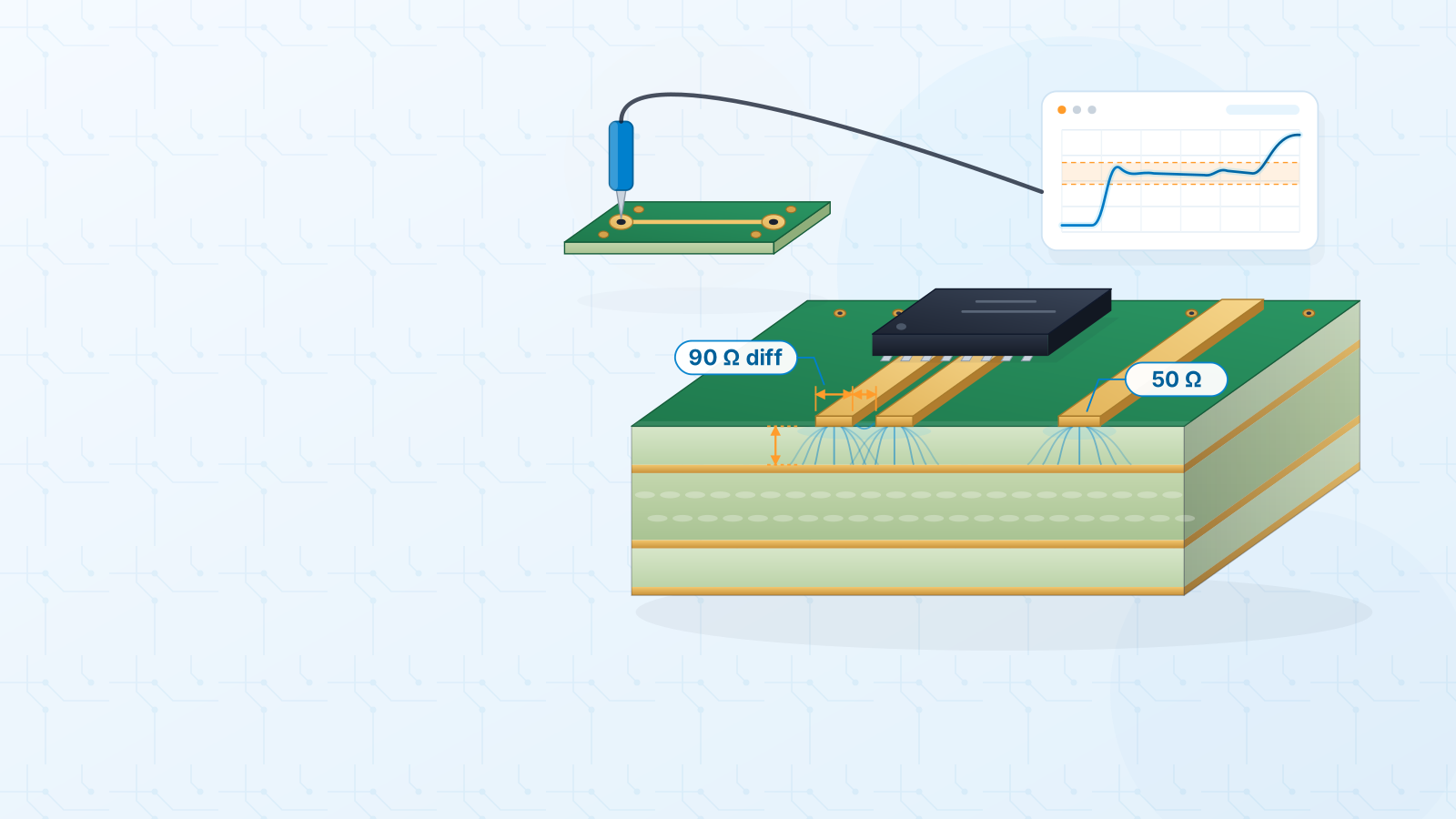
Controlled Impedance for First-Timers: Stack-up, Traces and What to Tell Your Fab
Adding USB, Ethernet, DDR or RF for the first time? Learn when impedance matters, what sets it, and how to write clear impedance notes for your fab.
15 Nov 2026 · 4 min read
 PCB Design
Designing a Flex PCB That Bends Without Cracking: A Checklist
Moving from rigid to flex? Most flex failures are mechanical. This checklist covers bend radius, routing in the bend, stiffeners, coverlay and when rigid-flex is worth it.
15 Nov 2026 · 5 min read
 PCB Design
9 DFM Mistakes That Hold Up Your First PCB Order
Most engineering queries on a first PCB order come from a few avoidable design and file mistakes. Here are nine of them and a quick checklist to catch them before upload.
15 Nov 2026 · 5 min read
 PCB Design
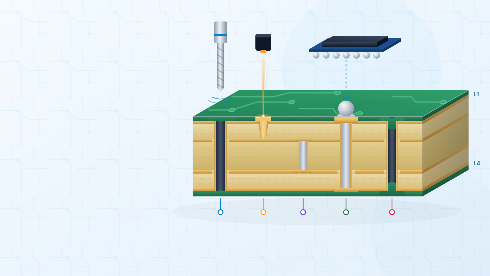
Through, Blind, Buried, Tented, Plugged: Vias Explained Without the Jargon
A plain-language tour of via types and covering options — through, blind, buried, microvia, tented, plugged, filled — and how to pick the simplest one your board actually needs.
15 Nov 2026 · 4 min read