10 Ways to Lower Your PCB Cost Without Hurting Quality
Board size, layer count, standard options, simple drilling and smart quantity choices move your PCB price the most. Ten practical tips to pay less without cutting corners.
Microplacer team · 15 November 2026 · 5 min read
 Ordering & Cost
Most of what you pay for a PCB is decided long before you open a calculator. It is decided in the layout tool, when you pick the outline, the layer count, the drill sizes and the finish. The good news: the choices that save the most money rarely cost you any reliability — they just stop you paying for things your board does not need.
Here are ten practical ways to bring the price down, starting with the ones that usually matter most.
1. Shrink the board outline: the biggest single lever
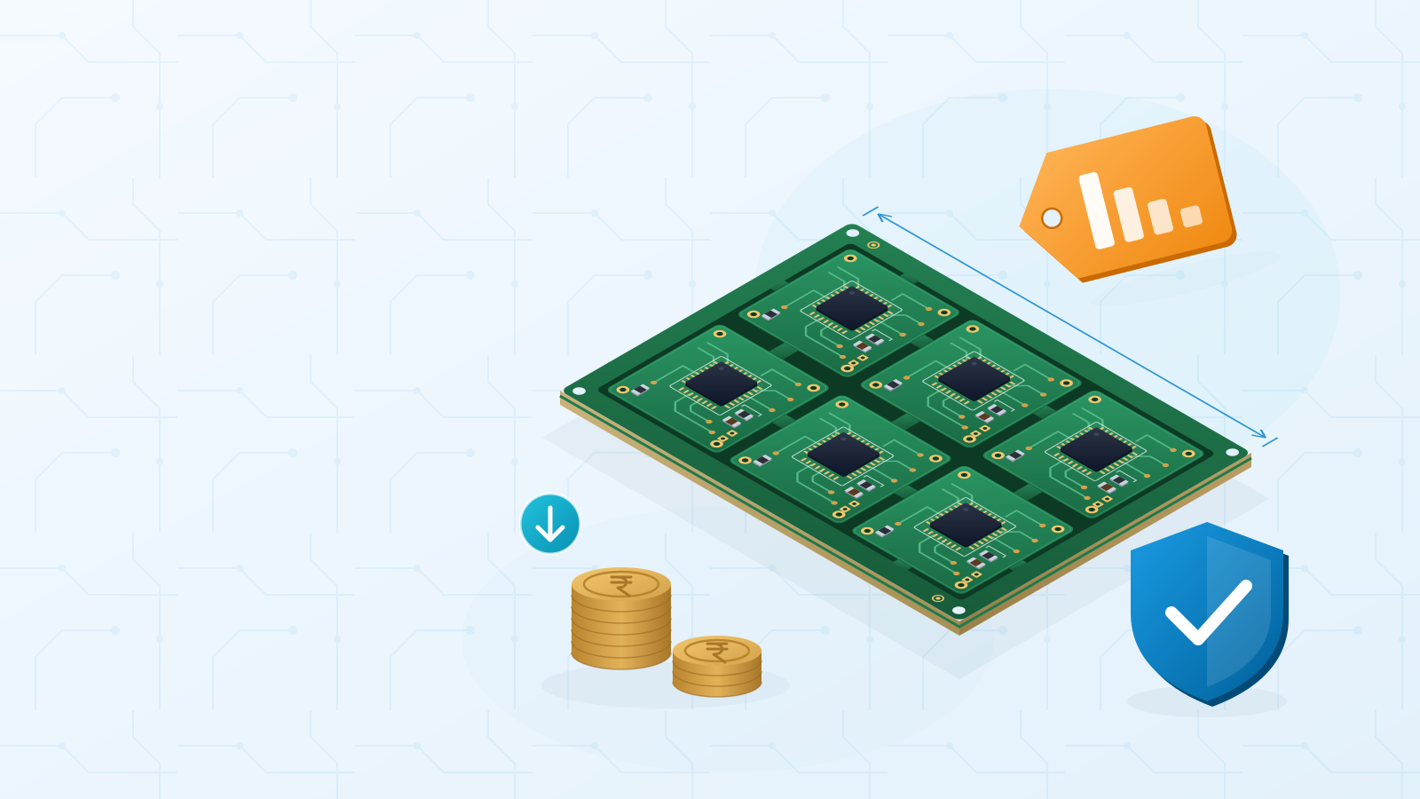
A bare board is priced largely on area. Every square centimetre means more laminate, more copper to image and etch, and more panel space that could have held another board. Before freezing the layout, check whether empty corners can go and connectors can move closer together.
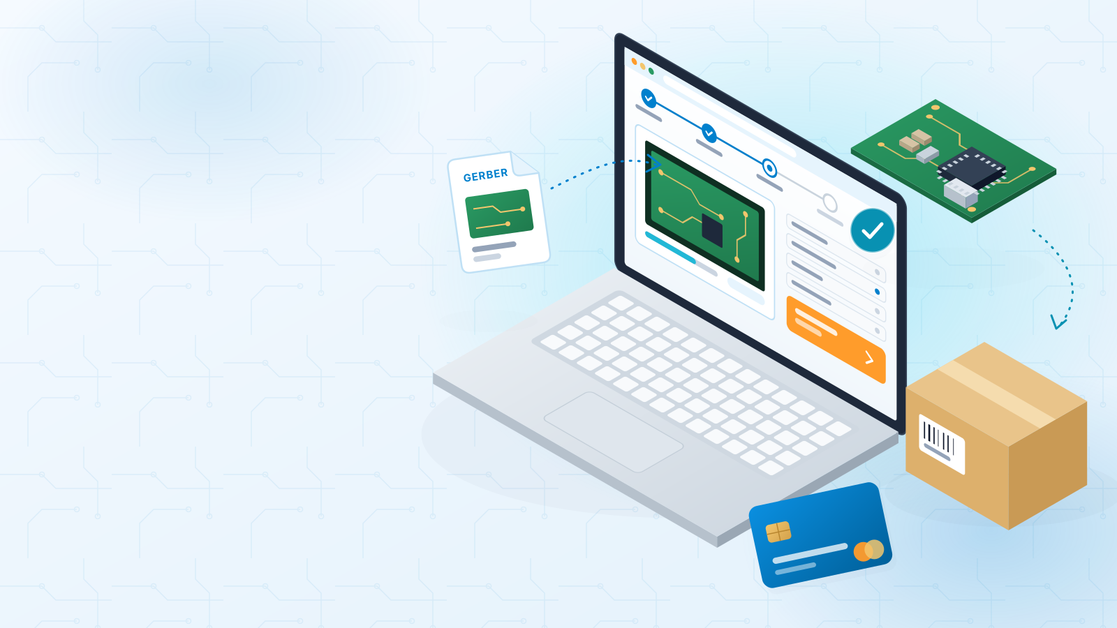
A simple rectangle also nests better on a production panel than an odd shape with long tabs. The board size is read automatically from the outline layer in your Gerber, so make sure that layer shows exactly one clean, closed outline — and confirm the size in the quote.
2. Choose the layer count honestly
One- and two-layer boards are the most economical, and each step up adds lamination, drilling and imaging work. When the circuit routes cleanly on two layers, there is no price argument for four.
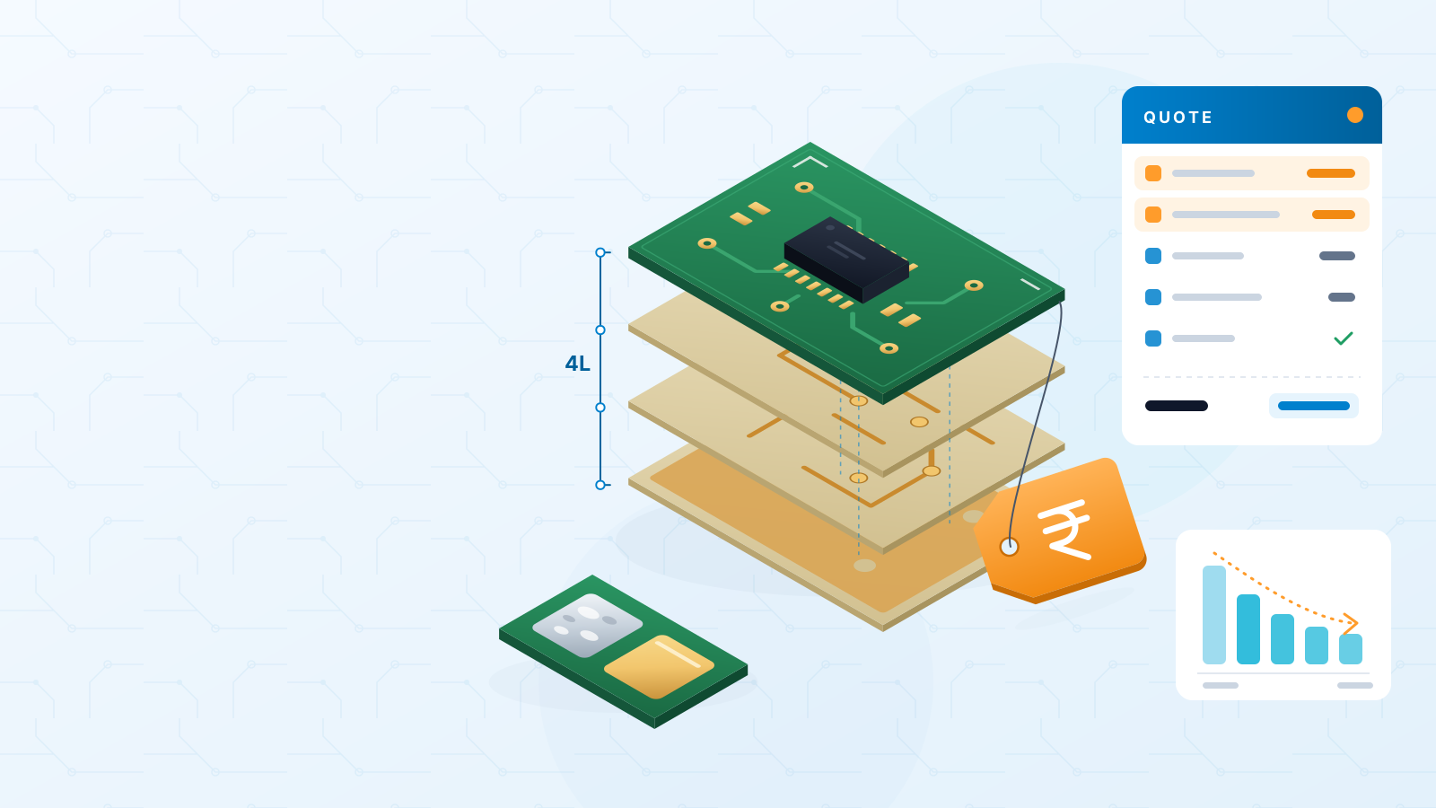
But do not force it. A crowded 2-layer board with a broken ground return and long detours often needs another revision. Moving to 4 layers with solid inner ground and power planes can make routing simpler, improve noise and EMI, and get you a working board on the first spin. Two extra layers that save one re-spin are the cheaper choice.
3. Stay with standard thickness, copper and finish
Standard options are the lowest cost and the quickest to produce. Change one only when the design truly demands it.
| Choice | Cost-friendly default | Pay more only when… |
|---|---|---|
| Material | FR-4 | You need high-frequency laminate, a metal core or flex. |
| Thickness | 1.6 mm | A connector, slot or enclosure needs a different value. |
| Outer copper | 1 oz | Traces must carry high current and widening them is not enough. |
| Surface finish | HASL or lead-free HASL | You use fine-pitch or BGA parts that need flat ENIG pads. |
For a RoHS product without very fine-pitch parts, lead-free HASL is usually enough. Keep ENIG for boards where pad flatness really matters, such as fine-pitch QFNs and BGAs.
4. Keep holes and vias ordinary
Drilling is a big share of the work on any board. A few habits keep it simple:
- Use a small set of drill sizes rather than many slightly different ones.
- Use normal through-hole vias where you can; very small vias and microvias need finer drilling and tighter process control.
- Choose tented vias (covered by solder mask) unless you need plugged or filled vias, for example via-in-pad under a BGA.
- Leave annular rings and clearances at comfortable values instead of the tightest the shop can do.
5. Skip tolerances and extras you do not need
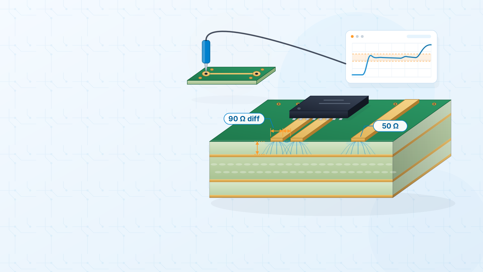
Tight outline tolerance, impedance control, castellated holes, gold fingers, edge plating and extra reports all solve real problems — and each one adds process steps. If you have no fast differential pairs, your enclosure has a few millimetres of play and the board does not plug into a slot, you can usually leave these off. For each option, ask: what fails if I untick this?
6. Use quantity breaks wisely
The minimum order is 5 PCBs. Checking the files, setting up the job and testing take roughly the same effort whether you order five boards or fifteen, so on a tiny order each board carries a big slice of that effort. Step up to the next quantity and the total often rises only a little while the price per board drops.
7. Plan assembly-friendly layouts early
If the boards will be assembled, cost starts at the layout too. The instant assembly price is worked out from the solder pads, and keeping all SMD parts on a single side spares the board a second paste-and-reflow cycle. Boards with BGA, LGA or 0201 parts go to engineering review, so for a quick prototype it is worth avoiding them where the design allows. Also make sure your parts list, placement file and silkscreen agree.
8. Run a clean DFM check before you order
The most expensive board is the one you make twice. Run your CAD tool's design rule check against the manufacturer's limits, then work through this list:
- 1All layers exported, with one closed board outline.
- 2Drill file included and aligned with the copper layers.
- 3Trace width, spacing and annular rings inside published limits, with some margin.
- 4Silkscreen kept off pads; polarity and pin 1 clearly marked.
- 5Production notes (thickness, finish, colour) written in a readme or fab layer.
Our engineers check files before production too, and compare your production notes with the options you chose.
9. Enter the right options up front
If the board size, layer count or finest via you select differs from your files, it will come up in the file check and slow things down. Upload your Gerber rather than typing a size: the size is read from the files automatically, and you just confirm it.
10. Remember the online price already includes GST and shipping
When you compare quotes, compare like with like. The online price for FR-4 and flex PCBs up to 16 layers already includes GST and express shipping within India, and 100% flying-probe electrical testing is free on every board. Bare PCBs typically arrive in 10–15 working days. A lower headline number can grow once tax, freight and testing are added.
Next step
Want the option-by-option detail? Read our PCB cost factors guide, check the limits on PCB capabilities, then upload your Gerber for an instant price. Questions about payment and delivery are answered in the online ordering FAQ.
#pcb-cost#design-for-cost#dfm#pcb-price#online-quote
Get an instant PCB quote